Expedition PCB Viewer: Simplify Your PCB Design Process! Pcb stack-up guide & examples
If you are looking for PCB PRO - Tutorials, Tips, and Tricks for using Cadence Schematic you've visit to the right page. We have 25 Images about PCB PRO - Tutorials, Tips, and Tricks for using Cadence Schematic like PCB Process Flow Chart | www.homillux.com, PCB Process Flow Chart | www.homillux.com and also PCB PRO - Tutorials, Tips, and Tricks for using Cadence Schematic. Read more:
PCB PRO - Tutorials, Tips, And Tricks For Using Cadence Schematic
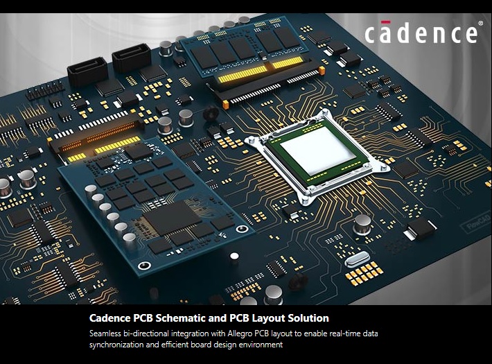 becomepcbpro.com
PCB PRO - Tutorials, Tips, and Tricks for using Cadence Schematic ...
Baru 10 Pcb Etching Process Simple Dan Minimalis
 skemasupergalaxy.blogspot.com
Baru 10 Pcb Etching Process Simple Dan Minimalis
How To Calculate PCB Design Cost? - RayPCB
 www.raypcb.com
How to calculate PCB design cost? - RayPCB
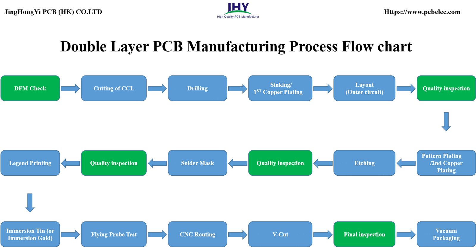
PCB Process Flow Chart | Www.homillux.com
 www.homillux.com
PCB Process Flow Chart | www.homillux.com
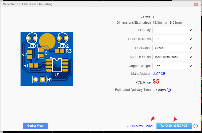
Free Pads Pcb Viewer - Newbuyer
 newbuyer100.weebly.com
Free Pads Pcb Viewer - newbuyer
Free Pcb File Viewer - Coachingpoo
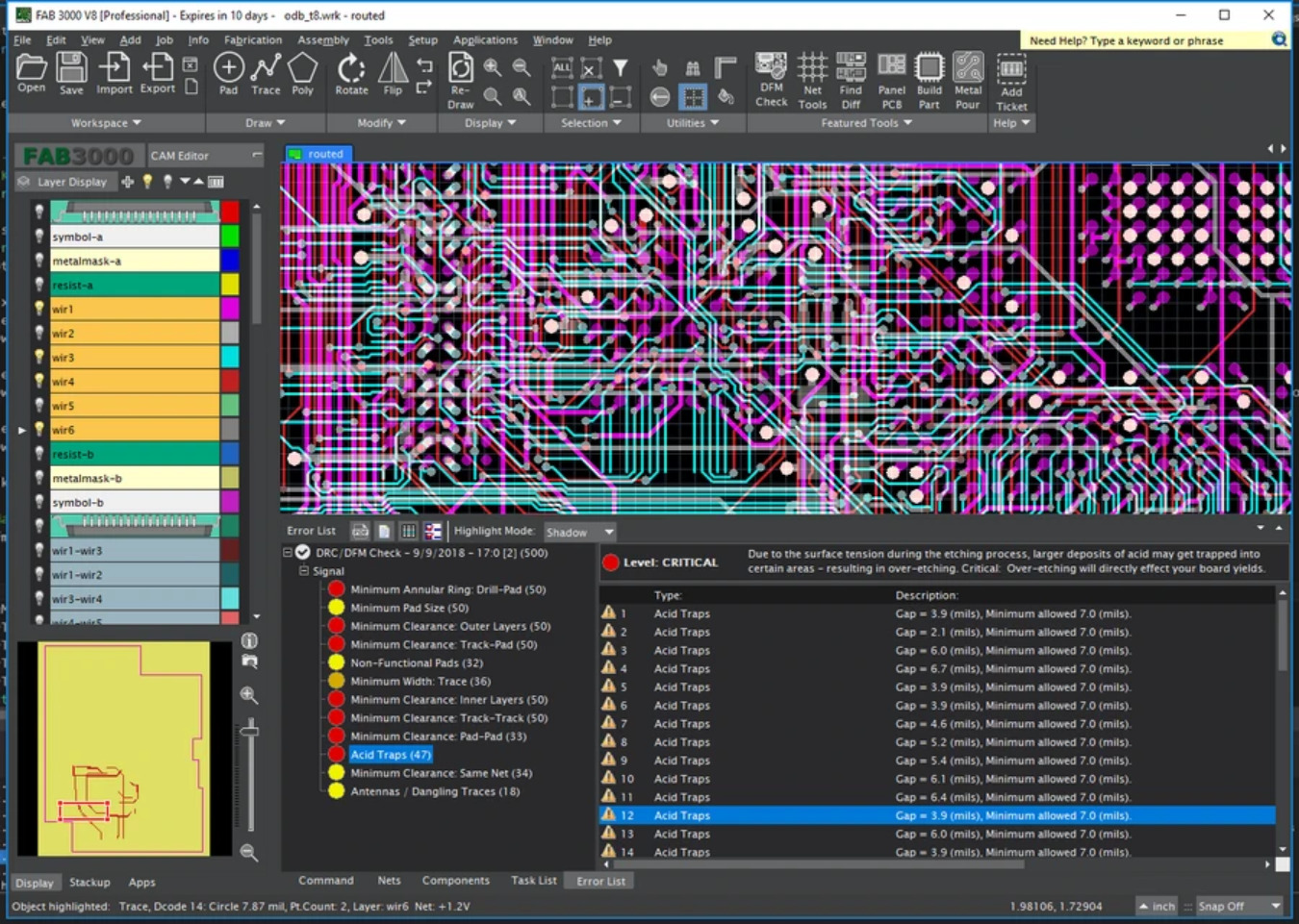 coachingpoo.weebly.com
Free pcb file viewer - coachingpoo
6 Layer Pcb Design Guidelines - Design Talk
 design.udlvirtual.edu.pe
6 Layer Pcb Design Guidelines - Design Talk
Mentor Graphics Expedition Pcb Free Download - Coolyload
 coolyload166.weebly.com
Mentor Graphics Expedition Pcb Free Download - coolyload
PCB Process Flow Chart | Www.homillux.com
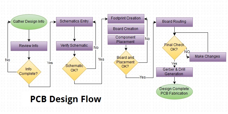 www.homillux.com
PCB Process Flow Chart | www.homillux.com
Process Concept Diagram Pcb Chemical Engineering The Pcb Des
 schematicvaradavi660.z21.web.core.windows.net
Process Concept Diagram Pcb Chemical Engineering The Pcb Des
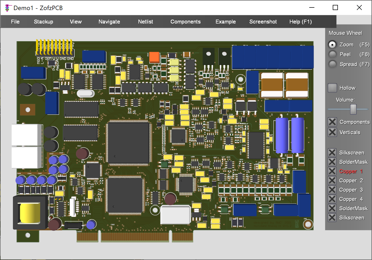
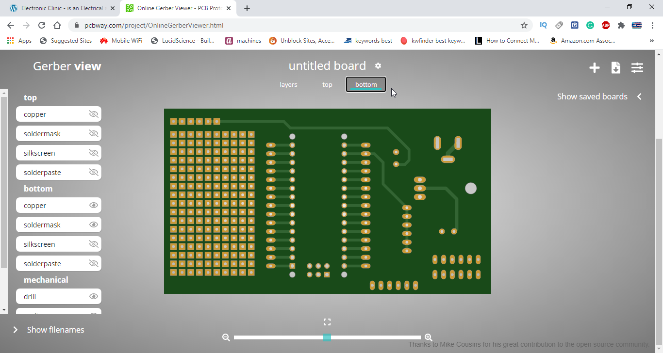
Pcb Viewer
 intpik.ru
Pcb viewer
How To Design A PCB Antenna?
 www.nextpcb.com
How to Design a PCB Antenna?
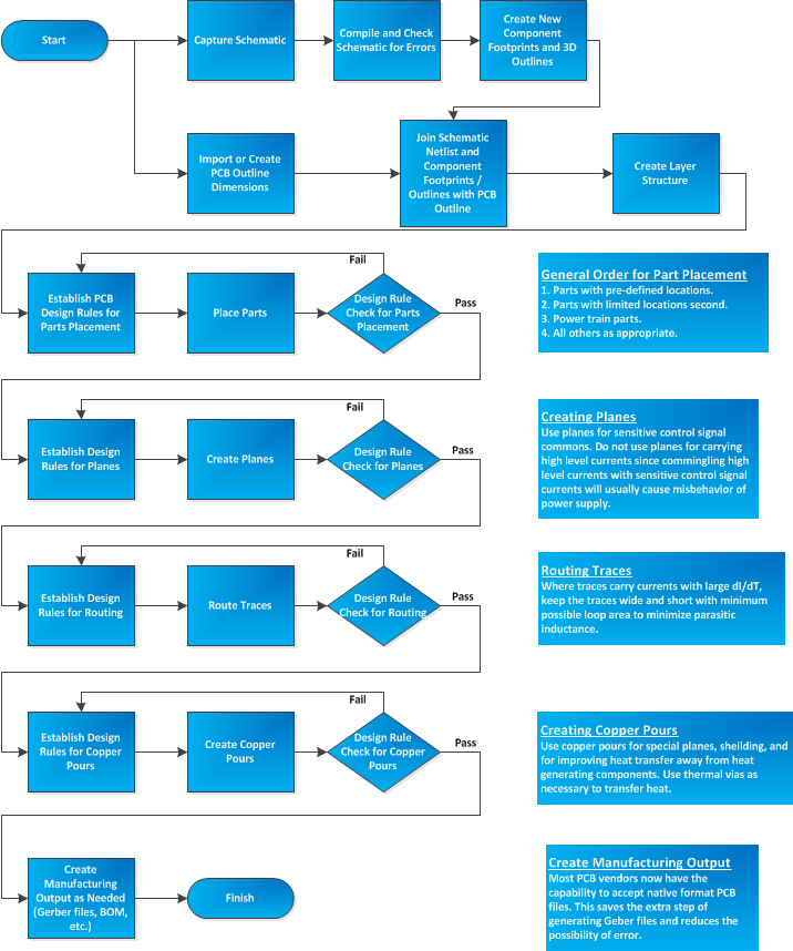
Basic Steps To Design A PCB Layout – PCB HERO
 www.pcb-hero.com
Basic Steps to Design a PCB Layout – PCB HERO
PCB Design Services | PCB Design Process | PCB Prototyping Process
 gambittq.com
PCB Design Services | PCB design Process | PCB Prototyping Process
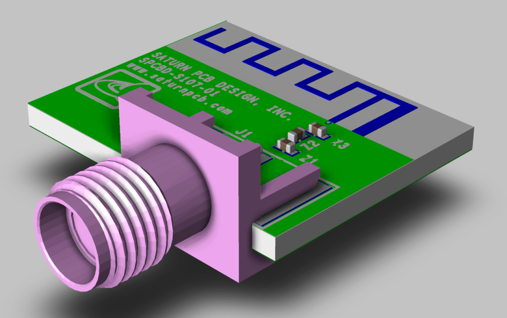
PPT - Simplify Your Design With Vertical Launch And Solderless PCB
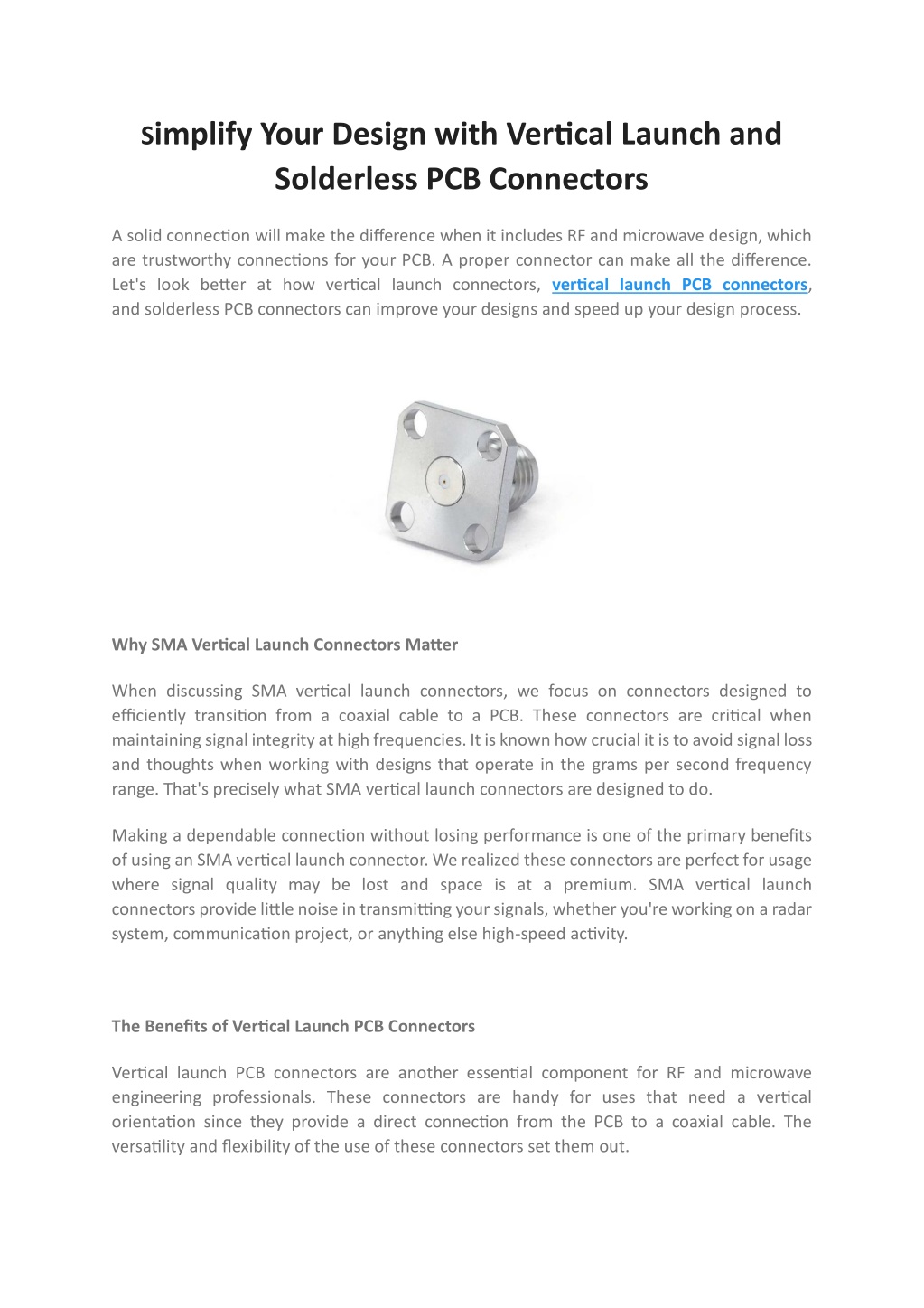 www.slideserve.com
PPT - Simplify Your Design with Vertical Launch and Solderless PCB ...
PCB Design Checklist To Build An Efficient Board | Sierra Circuits
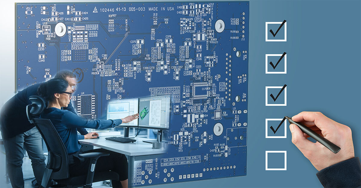 www.protoexpress.com
PCB Design Checklist to Build An Efficient Board | Sierra Circuits
PCB Stack-Up Guide & Examples | San Francisco Circuits
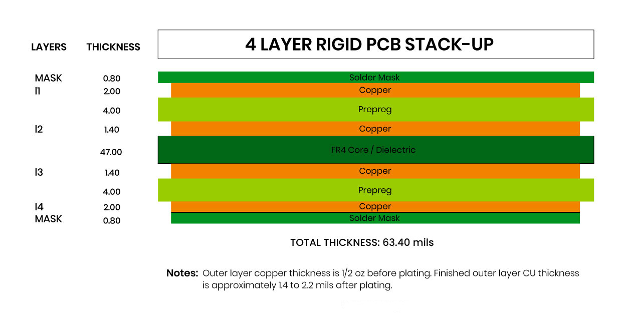 www.sfcircuits.com
PCB Stack-Up Guide & Examples | San Francisco Circuits
Pcb Viewer
 intpik.ru
Pcb viewer
How To Use A Modular Approach To Simplify Your PCB Design Process
 www.linkedin.com
How to Use a Modular Approach to Simplify Your PCB Design Process
SECO S.p.A.: Streamlining The PCB Design Process With SECO
 www.seco.com
SECO S.p.A.: Streamlining the PCB Design Process with SECO
Pcb Design Process Flow At Louise Whipple Blog
 storage.googleapis.com
Pcb Design Process Flow at Louise Whipple blog
PCB Process Flow Chart | Www.homillux.com
 www.homillux.com
PCB Process Flow Chart | www.homillux.com
Power Supply PCB Designer And Layout Expert
 www.power-supply-designer.com
Power Supply PCB Designer and Layout Expert
Pcb Viewer
 intpik.ru
Pcb viewer
Pcb Viewer
 intpik.ru
Pcb viewer
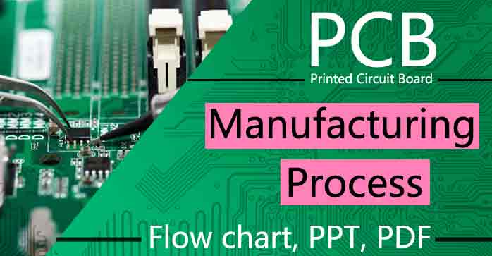
Pcb design checklist to build an efficient board. pcb design checklist to build an efficient board. Pcb process flow chart